Table of Contents
Problem Overview............................................................................................................... Page
2
Requirements and Specifications..................................................................................... Page
3
Mechanical............................................................................................................... Page
3
Electrical.................................................................................................................. Page
4
Environment............................................................................................................. Page
4
Documentation........................................................................................................ Page
5
Testing...................................................................................................................... Page
5
General..................................................................................................................... Page
6
Design Philosophy and Approach.................................................................................... Page
6
Deliverables and Schedule................................................................................................ Page
8
Design Section................................................................................................................. Page
10
Design
Summary.................................................................................................. Page
10
Digital
Design........................................................................................... Page
11
Schematics,
Diagrams, and Drawings.............................................................. Page
11
Analysis
and Simulation....................................................................................... Page
12
Tradeoff
and Design Decisions.......................................................................... Page
12
Parts
Description.................................................................................................. Page
13
Budget Section................................................................................................................. Page
14
Acceptance Document..................................................................................................... Page
16
Appendix A - Schematics and Simulations.................................................................. Page
A-0
Appendix B - Parts Information and Research............................................................ Page
B-0
Problem Overview
The device we are designing is a universal strain gauge amplifier. The strain gauge is simply a transducer and, therefore, will be simulated by feeding an analog signal as the input to the system. The resistance of a strain gauge changes as the surface it is mounted to experiences mechanical strain. Typically they are made from Silicon and used as force sensors. Since the signals from strain gauges are highly varied, our amplifier must have the capability of downloading configuration data to the amplifier in order to ensure that zero and span controls are not needed. The range of signals produced by the strain gauge can be simulated for this prototype unit.
The circuitry of the system consists of some op-amps,
a programmable gain amplifier (PGA), a 12-bit analog to digital converter
(ADC), and a digital to analog converter (DAC). A block diagram of this system is included in Figure 1.1
below.
The resistors simulate the strain gauge and provide a
range of signals to be fed into the system.
The op amp is then used to remove the DC offset into the system. By simulating the characteristics of a
strain gauge we are able to test the amplifier circuit without an actual strain
gauge device. After receiving the
signal from the strain gauge, the PGA sets the gain of the amplifier to x1, x2,
x4, or x8. The signal is then sent to
an ADC, which in turn feeds the converted data back to the microcontroller for
further analysis. The microcontroller
receives, through a serial communication port, the data for the gain stage, the
ADC, and the DAC. It sets the gain of
the PGA, calibrates the system via the DAC in the control loop, and tells the
ADC whether a digital or analog signal is required.
The focus of this project is to prototype the
amplifier system. The final product
would be customized by Dataforth to fit specific applications, due to the
variety of uses of strain gauges in industry.
Some examples in industrial processes that could utilize this amplifier
are steel processing, automobile manufacturing, airplane testing, etc.

Figure
1.1, System Diagram of Strain Gauge Amplifier.
Requirements and Specifications
Mechanical
This section describes the physical characteristics
of the entire system. The [DRY1]amplifier is, at this time, primarily a prototype; as
a result the mechanical aspects are not limited in size and weight. However, the entire circuit will be
constrained to the following dimensions, which will allow for greater
flexibility in both the manufacturing and design of the product.
- Size will be kept within
2ft width, 2ft length, and 2ft height.
- Weight will be
less than 20 pounds.
- The components will be
centralized fully on Vectorbord.
- The
interconnectivity of the components will be with wires and solder.
Electrical
This section contains the specifications for the electronic components and electrical interfacing of the system. It provides detailed characteristics of the individual components, as well as the general requirements for their interfacing.
·
Bandwidth is not
critical. However, it will be limited
to a maximum of 100Hz.
·
The PGA will have
preset gains of 1, 2, 4, and 8.
·
The resistors should be
rated at 1/4 watt and have a tolerance of 1 or 2%.
·
The bridge is powered
with a laboratory supply, adjustable from 1 volt to 10 volts.
·
The Microchip PIC
family PIC17C756 microcontroller will be used.
·
The microcontroller
communicates through a serial port with the computer and receives commands from
the host computer and sends data back in response.
·
The microcontroller
sets the gain of the PGA and loads the data into the DAC from the computer.
·
The DAC (D/A) provides
the analog signal to zero the bridge.
·
The data will be
displayed on the screen of the computer (PC).
Environment
This
section provides specifications on the environment that the system will operate
in. Since environment conditions will
vary greatly, depending on the use, these specifications must encompass a wide
range of possible scenarios.
- Must be able to
operate in environments of 0C to +55C.
- The system should
work under normal atmospheric conditions, with no vibration or shock to
the system.
Documentation
This
section provides a description of the documentation needed to properly operate
the system, as well as the functionality.
- A user’s guide for the
amplifier will be made available after the testing has been completed.
Testing
This
section discusses the processes for which testing will be implemented. It describes the conditions for which the
amplifier must satisfy.
- Simulation of strain
gauges through the use a four-resistor bridge of 3 100-ohm (±2%) resistors and a single resistance adjustable
from approximately 95 ohms to 105 ohms.
- Verify that the computer
sends commands to our system and receives back data through the serial
ports.
- Verify that the
microcontroller will calibrate the system.
- To check the accuracy of
the system, measure the input voltage with a digital voltmeter and compare
to the output.
General
This section provides general
requirements that the system must comply with.
The device will be used in various situations, each of which will
require its own unique set of specifications.
In order to accommodate this flexibility, the device will be designed to
allow the user to easily change the configuration of the device with minimal
problems.
- The system must not
need zero and span controls.
- The accuracy of the
system must be at least 0.1%.
- A simple control loop
should calibrate the system.
Design Philosophy and Approach
Our project has been broken down into different
modules. These modules are assigned to different team members. The team leader
is responsible for the system integration and is, therefore, involved with all
the individual modules assigned. The
modules are as follows:
-
Interfacing between
controller and system (I/O Bus)
-
Web page development
-
Documentation
-
Microcontroller coding
and implementation
-
DAC and ADC interfacing
and accuracy
-
PGA interfacing and
functions
-
Strain gauge simulator
-
System integration
We have broken down our project into different
categories assigning specific tasks to individual team members. The reason for this division of labor is to allow the individual to become highly
specialized in each area of interest to our project. This in turn implies that each individual on the team will play a
vital role in the outcome of the project due to the fact that final design is
an integration of each other’s contributions.
This also means that each member must perform in order to achieve
success.
In order to insure individual success, the team
leader will observe and obtain feedback from the individual members throughout
the process. Due to the knowledge of
the individual projects, it will also be the duty of the team leader to
supervise the final integration of the product after the completion of the individual
stages. Below is a breakdown of the
different applications the team members will take responsibility for.
This
listing is by no means limited to or exclusively for the individual assigned to
the task, but rather a responsibility for which they are accountable.
Our philosophy is to develop, on schedule, a
functioning, reliable system (microcontroller controlled strain gauge
amplifier) with accuracy that meets or exceeds specifications.
Deliverables
Project Proposal Dec. 13
Bill of Materials Dec. 13
Start Coding Jan. 25
Start Testing Feb. 10
System Integration Mar. 10
Final Testing Mar. 10
Complete Coding Mar. 14
Documentation Apr. 20
Prototype Presentation Apr. 28
Schedule
Task Duration Start Date End Date
|
Documentation |
142 days |
10/6/99 8:00 |
4/20/00 17:00 |
|
Test
Document |
58 days |
2/1/00 8:00 |
4/20/00 17:00 |
|
Linear/DSP |
120 days |
10/11/99 8:00 |
3/24/00 17:00 |
|
Web
Development Software |
40 days |
10/11/99 8:00 |
12/5/99 17:00 |
|
Digital
to Analog Converter |
38 days |
10/11/99 8:00 |
12/1/99 17:00 |
|
Analog to
Digital Converter |
38 days |
10/11/99 8:00 |
12/1/99 17:00 |
|
Programmable
Gain Amplifier |
38 days |
10/11/99 8:00 |
12/1/99 17:00 |
|
Strain
Gauge |
16 days |
10/11/99 8:00 |
11/1/99 17:00 |
|
Input/Output |
110 days |
10/11/99 8:00 |
3/10/00 17:00 |
|
Final MC
Code |
139 days |
10/11/99 8:00 |
4/20/00 17:00 |
|
MS
Project Plan |
4 days |
10/6/99 8:00 |
10/11/99 17:00 |
|
Design
Plan |
4 days |
10/6/99 8:00 |
10/11/99 17:00 |
|
Client
Satus Report |
3 days |
10/21/99 8:00 |
10/25/99 17:00 |
|
Draft
Proposal |
11 days |
11/8/99 8:00 |
11/22/99 17:00 |
|
Chip
Documentation |
19 days |
10/6/99 8:00 |
11/1/99 17:00 |
|
Final
Proposal |
1 day |
11/29/99 8:00 |
11/29/99 17:00 |
|
Proposal
Acceptance |
1 day |
12/6/99 8:00 |
12/6/99 17:00 |
|
Testing |
98 days |
11/25/99 8:00 |
4/10/00 17:00 |
|
Final
Test |
11 days |
3/27/00 8:00 |
4/10/00 17:00 |
|
Microcontroller
Test |
6 days |
3/14/00 8:00 |
3/21/00 17:00 |
|
SG
Simulation Test |
5 days |
11/25/99 8:00 |
12/1/99 17:00 |
|
Communication |
72 days |
10/11/99 8:00 |
1/18/00 17:00 |
|
Initial
Client Contact |
9 days |
10/12/99 8:00 |
10/22/99 17:00 |
|
Internal
Project Review 1 |
5 days |
10/11/99 8:00 |
10/15/99 17:00 |
|
Internal
Project Review 2 |
1 day |
1/18/00 8:00 |
1/18/00 17:00 |
|
Faculty Advisor
Meetings 1 |
1 day |
10/25/99 8:00 |
10/25/99 17:00 |
|
Faculty
Advisor Meetings 2 |
1 day |
10/27/99 8:00 |
10/27/99 17:00 |
|
Faculty
Advisor Meetings 3 |
1 day |
11/8/99 8:00 |
11/8/99 17:00 |
|
Faculty
Advisor Meetings 4 |
1 day |
11/29/99 8:00 |
11/29/99 17:00 |
|
Faculty
Advisor Meetings 5 |
1 day |
12/2/99 8:00 |
12/2/99 17:00 |
|
Communication
with client 1 |
5 days |
10/18/99 8:00 |
10/22/99 17:00 |
|
Communication
with client 2 |
1 day |
11/30/99 8:00 |
11/30/99 17:00 |
|
Hardware |
15 days |
11/22/99 8:00 |
12/10/99 17:00 |
|
Component
Selection |
15 days |
11/22/99 8:00 |
12/10/99 17:00 |
|
Software |
125 days |
10/11/99 8:00 |
3/31/00 17:00 |
|
Microcontroller
Programming |
125 days |
10/11/99 8:00 |
3/31/00 17:00 |
|
Demonstration |
1 day |
4/28/00 8:00 |
4/28/00 17:00 |
|
Design
Conference |
1 day |
4/28/00 8:00 |
4/28/00 17:00 |
|
Final
Demonstration |
1 day |
4/28/00 8:00 |
4/28/00 17:00 |
|
Presentation |
20 days |
10/11/99 8:00 |
11/5/99 17:00 |
|
Class
Presentation #1 |
1 day |
10/11/99 8:00 |
10/11/99 17:00 |
|
Class
Presentation #2 |
1 day |
11/5/99 8:00 |
11/5/99 17:00 |
|
Purchasing |
2 days |
12/10/99 8:00 |
12/13/99 17:00 |
|
Bill of
Materials/Purchased |
2 days |
12/10/99 8:00 |
12/13/99 17:00 |
|
Promotion |
23 days |
10/14/99 8:00 |
11/15/99 17:00 |
|
Web Page |
23 days |
10/14/99 8:00 |
11/15/99 17:00 |
|
Complete
Members Page |
7 days |
10/14/99 8:00 |
10/22/99 17:00 |
|
Project
Desription |
7 days |
10/14/99 8:00 |
10/22/99 17:00 |
|
Project
Schedule |
12 days |
10/21/99 8:00 |
11/5/99 17:00 |
|
Post
Documents |
12 days |
10/21/99 8:00 |
11/5/99 17:00 |
|
Advertise
Web Page |
12 days |
10/29/99 8:00 |
11/15/99 17:00 |
|
Project
Control |
11 days |
11/22/99 8:00 |
12/6/99 17:00 |
|
Cost
Analysis |
8 days |
11/22/99 8:00 |
12/1/99 17:00 |
|
Proposal
Submission |
1 day |
11/29/99 8:00 |
11/29/99 17:00 |
|
Proposal
Approval |
1 day |
12/6/99 8:00 |
12/6/99 17:00 |
|
Research |
37 days |
10/11/99 8:00 |
11/30/99 17:00 |
|
I/O
Interface |
26 days |
10/11/99 8:00 |
11/15/99 17:00 |
|
Linear/DSP |
37 days |
10/11/99 8:00 |
11/30/99 17:00 |
|
Programmable
Gain Amplifier |
26 days |
10/11/99 8:00 |
11/15/99 17:00 |
|
Digital
to Analog Converter |
26 days |
10/11/99 8:00 |
11/15/99 17:00 |
|
Analog to
Digital Converter |
26 days |
10/11/99 8:00 |
11/15/99 17:00 |
|
Microcontroller |
16 days |
10/11/99 8:00 |
11/1/99 17:00 |
|
Travel |
1 day |
11/12/99 8:00 |
11/12/99 17:00 |
|
Tucson
trip to Dataforth |
1 day |
11/12/99 8:00 |
11/12/99 17:00 |
|
|
|
|
|
Design
Section
Design Summary
Analog Design
The analog portion of the system
consists of a resistor network for simulation of a strain gauge, and a differential
amplifier with a set gain of 100, for adjusting the output of the strain gauge
into a more workable range (See Appendix A for schematics and simulation
data). Two voltage divider circuits
simulate the strain gauge; both powered by the same supply voltage adjustable
from 1 to 10 volts. The outputs of the
voltage divider circuits are independent of each other.
The first division provides a reference voltage
feeding into the negative terminal of the amplifier. The other voltage divider output is adjusted, through a digital
to analog converter (DAC), to match as closely as possible the voltage at the
positive input of the amplifier to the reference voltage at the negative input
of the amplifier.
By adjusting the inputs of the amplifier to match we
eliminate the difference between the terminals and obtain a common mode input
scenario, therefore producing no output signal from the amplifier. After the DAC has zeroed the bridge, we
adjust the potentiometer in the voltage divider circuit, which in turn changes
the reference voltage at the negative input of the amplifier. The difference between the two terminals
will be varied from 12.8 mV to 128 mV.
The adjusted difference in voltage simulates a strain being placed on a
gauge after it has been calibrated or zeroed.
Digital Design
The digital section of the system consists of 4
distinct parts: a Microcontroller, an Analog to Digital Converter (ADC), a
Digital to Analog Converter (DAC) and a Programmable Gain Amplifier (PGA).
The microcontroller sets the voltage
level for the op-amp in the analog section through a DAC, which in turn zeroes
the system. After receiving the signal from the strain gauge, the PGA sets the
gain of the amplifier to x1, x2, x4, or x8.
The signal is then sent to an ADC, which in turn feeds the converted
data back to the microcontroller for further analysis. The microcontroller receives, through a
serial communication port, the data for the gain stage, the ADC, and the DAC. It sets the gain of the PGA, calibrates the system
via the DAC in the control loop, and tells the ADC whether a digital or analog
signal is required.
Schematics, Diagrams and Drawings
A Block Diagram of the overall
system is shown in Figure 1.2, below.
The Strain Gauge Simulator and Differential Amplifier are shown
configured together in the schematic located in Appendix A, page A-8, creating
the analog portion of the design.
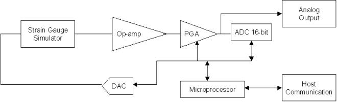 Figure 1.2, Block Diagram of the System
Analysis and Simulation
PSpice simulations were run to
verify the functionality of the differential amplifier and the strain gauge
simulator both individually and collectively.
Appendix A, pages A-1 – A-4, show the schematic and simulation results
from the strain gauge simulator, while pages A-5 – A-7, in Appendix A, show the
schematic and results from the differential amplifier simulation. Also found in Appendix A, on pages A-9 –
A-13, are the results of the combined system of the strain gauge simulator and
the differential amplifier. The results
clearly state that the circuit should function as anticipated.
An actual simulation was done in
addition to verify the functionality of the circuit and agreed with the
computer simulation results. The
experimental circuit used 5% tolerant resistors and a 25-ohm potentiometer but
provided accurate enough results to confirm proper design and operation of the
analog portion of the design.
Tradeoff and Design Decisions
Initially, there was indecision over
using parallel versus serial mode interactions between the microcontroller and
the ADC, DAC and the PGA. However, after learning that parallel interfacing was
possible by using two 8-bit I/O ports from the microcontroller, the idea of
using serial interface was discarded.
The use of 16 bit digital parts was decided upon in
order to meet the design specification of 0.1% accuracy. 16 bits provide a safe margin for noise and
bit swamping while maintaining accurate results. It was also decided that a 100-ohm potentiometer would be used in
order to simulate a greater input voltage range. This extended range allows for worst-case testing to be
performed.
Another issue is the operating speed
of the microcontroller. In order to keep the noise to a minimum, the
microcontroller needs to be run at a speed as low as possible. However, care
needs to be taken that the microcontroller is not run at a speed below what is
necessary to effectively read the required bandwidth of the system. Although
this is a consideration, it is not of primary concern. Clock speed noise is minimal in comparison
to other noise issues within the system.
Ground planes will be used to
further reduce noise by reducing the size of induced current loops. However,
the primary source of noise in our system will be the proximity of the analog
section to the digital section. This problem will be solved by physically
separating the two sections and connecting them at one, and only one, point for
cross-communication. Furthermore, the
reduction of noise in the system will continue to be of primary concern for
design decisions.
Parts Description
All resistors are rated for ¼ Watt
and have tolerances of 1%. The
potentiometer has a range of up to 100 Ohms.
The operational amplifier will be a high performance LM741. In order to reduce noise, Vectorbord containing
a ground plane will be used to mount the components. A mini Bud Box will also be used to enclose the circuit,
therefore protecting it from elements as well as providing further shielding
from noise.
The
microcontroller used will be the EPROM-based PIC17C756. The ADC will be16-bit integrating type for
better accuracy. The DAC will also be 16-bit.
A full description of the parts used may be found in Appendix B.
Budget Section
Part Number Description Qty Price Vendor
100XBX-ND 100 Ohm 1/4W 1% Axial 10 $1.08 Digi-Key
Metal Film Resistor
2.00KXBX-ND 2000 Ohm 1/4W 1% Axial 5 $0.54 Digi-Key
Metal Film Resistor
10.0KXBX-ND 10000 Ohm 1/4W 1% Axial 5 $0.54 Digi-Key
Metal Film Resistor
LM741CN-ND High Performance Operational 1 $0.56 Digi-Key Amplifier
V1009-ND P Bord/ 8.5 X 17”/ Copper Clad 1 $23.81
Digi-Key 1
side
V1056-ND Pad Cutter Tool with Handle 1 $20.90
Digi-Key
V1069-ND Microklip T42-1/C terminal 2 $10.64
Digi-Key
100 Count Package
V1101-ND Insertion Tool for Microklip 1 $18.10
Digi-Key
91F709 Minibox Housing 1 $22.82 Newark Electronics
318230 6ft serial db25m/db25f 1 $4.99 Insight
ADS7805P-ND IC 16 Bit A/D 28-DIP.3” 1 $31.90 Digi-Key
PGA203KP-ND IC Prog Gain Instr Amp 14 DIP 1 $11.02 Digi-Key
DAC712P-ND IC 16 Bit D/A Conv. 28 DIP.3’ 1 $18.72 Digi-Key
The estimated cost of
the prototype unit is $165.62. The
estimated cost of a production unit, excluding the printed circuit board and
housing, is approximately $30. Rob Cote
at Northern Arizona University will supply a computer for coding and
development of the mircocontroller, at an estimated cost of $500 for the
computer system. We will attempt to
obtain a microcontroller development package donation through Microchip's
University Program-Systems. If we are
unable to obtain these tools free of cost, Dataforth will purchase and provide
the necessary tools. We will provide a
bill of materials to Dataforth for the other components of the system and
Dataforth will purchase and provide the necessary materials by February 1,
2000. This is the payment arrangement
discussed and agreed upon.
Acceptance Document
This agreement sets forth the terms and
conditions for your use of this design.
We
agree that YOU shall be the patent proprietor in all patentable inventions of
every kind and description created or developed with regard to this design.
DISCLAIMER
OF WARRANTY
You
agree that your use of any part of this design and our services, and other data
and information is provided on an “AS IS” BASIS. EXCEPT AS EXPRESSLY SET FORTH
HEREIN, ALL CONTENT, SOFTWARE, HARDWARE, FUNCTIONS, SERVICES, MATERIALS AND
INFORMATION MADE AVAILABLE OR OTHERWISE PROVIDED, IS PROVIDED AS IS, WITHOUT
WARRANTIES OF ANY KIND, EITHER EXPRESS OR IMPLIED. WE EXPRESSLY DISCLAIM ANY
WARRANTIES OF ANY KIND, INCLUDING, BUT NOT LIMITED TO, WARRANTIES OF TITLE OR
IMPLIED WARRANTIES OF MERCHANTABILITY, FITNESS FOR A PARTICULAR USE OR PURPOSE,
TITLE, COMPATABILITY, SECURITY, ACCURACY, AVAILABILITY, DESIGN, CAPABILITY,
SUFFICIENCY, COMPLETENESS, OR NON-INFRINGEMENT. TO THE FULLEST EXTENT
PERMISSIBLE BY LAW, WE MAKE NO WARRANTIES AND SHALL NOT BE LIABLE FOR THE USE
OF THE DESIGN UNDER ANY CIRCUMSTANCES, INCLUDING BUT NOT LIMITED TO NEGLIGENCE
BY WE. DO NOT WARRANT THAT THE SOFTWARE, HARDWARE, FUNCTIONS, SERVICES,
MATERIALS AND INFORMATION MADE AVAILABLE OR OTHERWISE PROVIDED, CONTAINED IN
THE SITE OR SERVICES WILL BE UNINTERRUPTED OR ERROR-FREE, THAT DEFECTS WILL BE
CORRECTED, THAT THE SITE OR SERVICES WILL MEET ANY PARTICULAR CRITERIA OF
PERFORMANCE OR QUALITY, OR THAT THE SITE, INCLUDING FORUMS OR THE SERVER(S) ON
WHICH THE SITE IS OPERATED, ARE FREE OF VIRUSES OR OTHER HARMFUL COMPONENTS.
Neither WE or anyone else involved in creating, producing or delivering
services shall be liable for any direct, indirect, incidental, special or
consequential damages arising out of the use or inability to use this design.
LIMITATION
OF LIABILITY
USE OF THE DESIGN IS AT YOUR OWN RISK. YOU ASSUME FULL RESPONSIBILITY AND RISK OF LOSS RESULTING FROM YOUR DOWNLOADING AND/OR USE OF FILES, INFORMATION, COMMUNICATIONS, CONTENT, OR OTHER MATERIAL (INCLUDING WITHOUT LIMITATION SOFTWARE) ACCESSED THROUGH OR OBTAINED BY MEANS OF THE SITE. UNDER NO CIRCUMSTANCES SHALL WE BE LIABLE FOR ANY INDIRECT, PUNITIVE, SPECIAL, OR CONSEQUENTIAL DAMAGES THAT ARE DIRECTLY OR INDIRECTLY RELATED TO THE USE OF, OR THE INABILITY TO USE, THE SITE OR SERVICES, EVEN IF WE HAVE BEEN ADVISED OF THE POSSIBILITY OF SUCH DAMAGES. THE TOTAL LIABILITY OF US HEREUNDER IS LIMITED TO THE AMOUNT, IF ANY, ACTUALLY PAID BY YOU TO US, WHICH IS ZERO. YOU HEREBY RELEASE US FROM ANY AND ALL OBLIGATIONS, LIABILITIES AND CLAIMS.
WITNESS
my hand and seal this day of , 19 .
ACCEPTED
FOR US
By:
Date:
Name Greg Sitrick
By:
Date:
Name Vishal Golia
By:
Date:
Name Scott Hancock
By:
Date:
Name Donnie
Yazzie
ACCEPTED
FOR YOU
By:
Date:
Name Lee
Payne